Are you looking for a company that can provide you with the best Fast Print PCB products? Do you need someone to increase the value of the product significantly during the assembly process? Do you need time to participate in the layout review? This article serves as a guide to help you make informed decisions and achieve the desired results.
Among the key subjects on Fast Printing PCB include:
What is a Fast Print PCB?
This section gives a brief overview of the rapid printing PCB differing from the traditional manufacturing in terms of the steps involved, all necessary aspects and processes are pre-established.

Fast Print PCB Classification
This section introduces Pattern classes, and drill classes are used as shorthand terms to measure the manufacturability of the PCB. The smallest production tool size on the board is what determines the drill class.
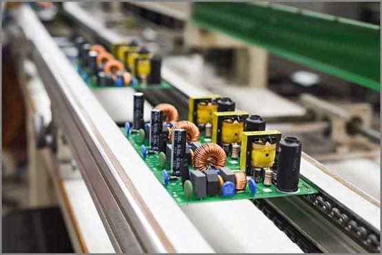
Factors Affecting the Quality of Fast Printing PCBs
This section details the rapid printing PCB inspection is a critical task that completed before forwarding it to the production stage, the faster, the better.
Factors to consider in fast-print PCB design
This section highlights the factors that need to considered when creating a high-quality, fast-print PCB design:
- Board Materials
- The Fast Print PCB Stack-up
- Copper Traces
- Vias
- Selection of Parts
- Signal and Power Integrity
Fast Print PCB Data Input Requirements
This section provides an in-depth description of the data input in the fast print PCB, several requirements that must meet.
Fast Print PCB in the data input, must meet several requirements. The acceptable data format for PCB layout has two main branches: artwork, and drill holes. The artwork has to do with all types of layers, for instance, copper, legend, and solder mask.
There are also peel off layers, SMD pastes layers and carbon layers not forgetting mechanical layers among many others. All Gerber specifications, dynamic process format, and CAD data are acceptable in terms of artwork.
In terms of drilling, some manufacturers will require only ASCII-encoded files because they are easy to read. What else is needed?
- Gerber format true drill data
- DPF(dynamic process format) true drill data
- Excellent 1 or 2 and an appropriate tool list that is appropriately embedded
- Sieb & Meyer and an appropriate tool list also appropriately embedded
We have already looked at two of the preferred data formats:
Extended Gerber X2 for artwork and Excellon 1 and an appropriate tool list embedded accordingly for drilling. Automated analysis and visualization also require a PCB visualizer. This visualizer works only with specifics such as mentioned above.
You should only provide the PCB manufacturer with the data files needed for production. One of these data files are the Gerber files which work with several layers like SMD paste, copper, solder mask, mechanical, peel-off and via-fill, and carbon.
Excellent, as mentioned before, works well when it comes to drilling. If you would like something different like an array biscuit or matrix from one board data, then you can supply your manufacturer with a (DPFdynamic process format) file or Gerber file.
It is easy, so make sure your file system has an easy-to-call name. Avoid long names. The best way to name a file is to match the name with the functionality. There should be information about the layer function. The data should not be scaled.
The Gerber files you supply should not contain zero size apertures, and the same is true for the Excellon data. It is either you are using a similar offset for the Gerber layers and the Excellon drill data or use no offset at all. Deal with the same units in all output files so that you do away with errors due to converting or rounding off.
The data supplied should be as seen from top to bottom through the PCB. It is the accepted universal practice. So what does this mean? It means that when you are looking at the Gerber data, the text on the top side of the board should be readable white text on the bottom should be non-readable. To minimize or eliminate mirroring errors, make sure the copper layer contains some small text. This text could be the company name or the board identification.
Use flashed pads for the Gerber files. The CAD PCB design software should have an aperture list to ensure the output reveals the apertures included in the design. All layers must come with the board outline, so us to enable your manufacturer to align all layers properly.
Therefore, to obtain high-quality fast-printing PCBs, you must find a professional supplier with extensive experience and professional materials and machines.
At OurPCB, they ensure that excellence is the epitome of all our operations. They specialize in Fast Print PCB production, among other PCB related services. For the last ten years, they have been in the business of providing a wide array of clients with critical and high-performance PCB and PCBA solutions.
Related Articles
- What Is 3D Printer Engraving?
- 3D Printing vs. CNC Machining: What’s the Difference?
- How to Print a File from Thingiverse (The Easy Way!)
- Do 3D Printers Use a Lot of Power? (The Numbers Inside)
Make sure you check out our YouTube channel, and if you would like any additional details or have any questions, please leave a comment below or join us on Discord. If you liked this article and want to read others click here.